IBM conducted experiments to grow semiconductor crystals in the microgravity environment of the ISS.
Traditional methods of growing semiconductor crystals on Earth often result in imperfections that can degrade the performance of electronic devices.
Microgravity allows for the growth of larger and more uniform semiconductor crystals with fewer defects. This leads to higher quality materials that enhance the performance and reliability of electronic devices.
The space-grown semiconductor crystals showed significant improvements in uniformity and purity, which could lead to the development of more efficient and powerful electronic devices. This research demonstrates the potential of space-based manufacturing to revolutionize the semiconductor industry.
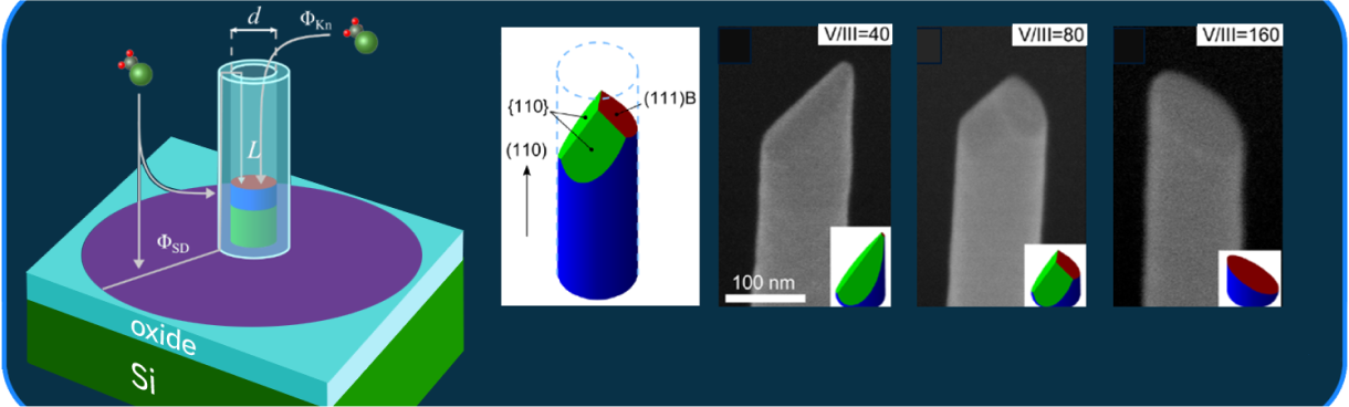
NASA researchers studied the growth of gallium nitride (GaN) crystals in microgravity, a material widely used in LEDs and power electronics.
GaN crystals grown on Earth often contain defects that limit their efficiency and lifespan.
Microgravity conditions facilitate the growth of defect-free GaN crystals, improving their electrical and thermal properties. This is crucial for the performance and durability of devices such as LEDs and power transistors.
The space-grown GaN crystals exhibited fewer defects and enhanced properties, leading to more efficient and reliable electronic devices. This advancement supports the broader adoption of GaN-based technologies.
Intel conducted experiments to explore the precision of nanofabrication processes in microgravity.
Nanoscale manufacturing on Earth is limited by gravity, which can cause imperfections and reduce the precision of semiconductor devices.
Microgravity allows for greater control over nanoscale fabrication processes, resulting in more precise and reliable semiconductor devices. This is essential for the development of advanced technologies such as quantum computing.
Process Silicon Carbide (SiC) semiconductor substrates in microgravity and evaluate defect reductions, as compared to Earth-processed SiC. The project team hopes to eventually commercially process SiC substrates, in LEO. SiC is a semiconductor material for power electronic use, but current applications are limited due to substrate defect levels.
The need for high-quality, defect-free semiconductors that enhance performance while reducing energy consumption.
Microgravity and vacuum conditions in space allow for the creation of semiconductors with superior performance and reduced defects. Space Forge’s manufacturing process can result in 10x to 100x performance improvements, reducing energy consumption by over 50%. This can lead to significant cost savings and environmental benefits, such as reducing CO2 emissions by 75%.
Demand is high for a better SiC wafer. SCM predicts that micorgravity report predicts that microgravity processing could add $1B in values to the SiC Semiconductor device market by 2020.
Researchers at the University of Florida studied the reduction of defects in silicon crystals grown in microgravity.
Silicon crystals grown on Earth often contain defects that impact the efficiency of semiconductor devices.
The microgravity environment minimizes the formation of defects in silicon crystals, resulting in higher quality materials. This improvement is critical for the performance and reliability of semiconductor devices used in a wide range of applications.
The space-grown silicon crystals exhibited significantly fewer defects, leading to enhanced performance and efficiency of semiconductor devices. This research underscores the potential of space-based manufacturing to improve the quality of semiconductor materials.
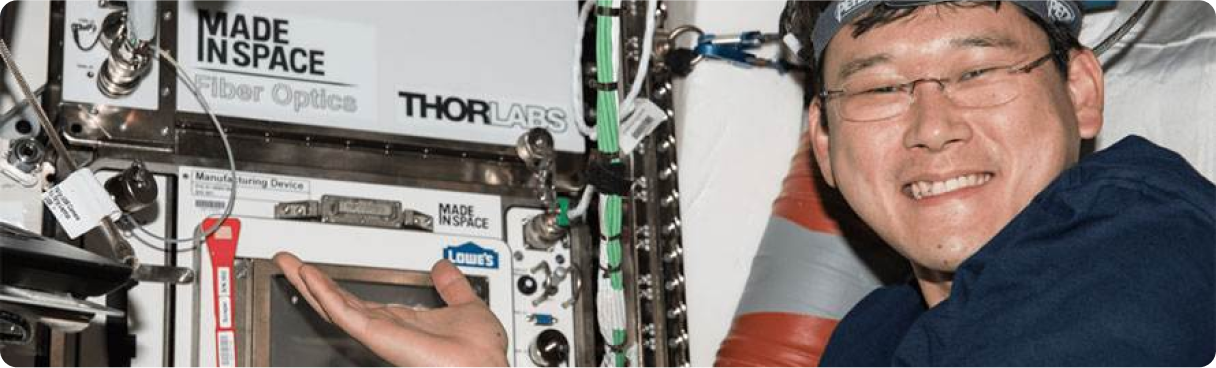
Manufacture high-quality ZBLAN optical fibers onboard the ISS. Microgravity production is expected to reduce imperfections, thereby improving the capabilities of the fibers. Project team believes that LEO-production of ZBLAN optical fibers is economically feasible and may present itself as the first in-orbit optical fiber manufacturing applicationProblem Solved on Earth: Silicon crystals grown on Earth often contain defects that impact the efficiency of semiconductor devices.
Reduce imperfections and increasing material properties (temperature, stress, etc)
The microgravity environment minimizes the formation of defects in silicon crystals, resulting in higher quality materials. This improvement is critical for the performance and reliability of semiconductor devices used in a wide range of applications.
Space based ZBLAN has superior properties and can be produced in a cost effective way for the last mile and specialty fiber markets